- 您现在的位置:买卖IC网 > Sheet目录538 > ZNBG3115Q20TC (Diodes Inc)IC SW 3BIAS TONE H/V 2.2V 20QSOP
�� �
�
�ZNBG3115�
�ZNBG3116�
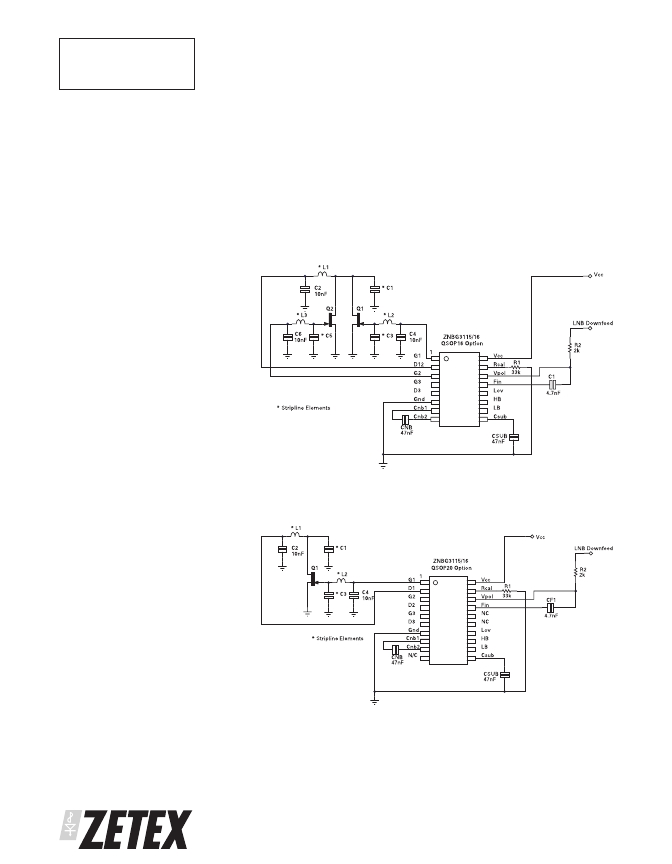
�APPLICATIONS� CIRCUIT�
�The� diagrams� below� show� partial� application� circuits� for� the� ZNBG� series� showing� all� external� components�
�required� for� appropriate� biasing.� The� bias� circuits� are� unconditionally� stable� over� the� full� temperature� range� with�
�the� associated� FETs� and� gate� and� drain� capacitors� in� circuit.�
�To� minimise� board� space� the� ZNBG3115/3116� is� offered� in� a� QSOP16� package.� To� reduce� the� pin� count� Drain� 1�
�and� Drain� 2� have� been� internally� connected.� This� is� possible� because� only� one� of� the� two� bias� stages� can� biased� at�
�one� time.The� QSOP16� offers� a� 40%� reduction� in� size� over� the� QSOP20� version.�
�Capacitors� C2� and� C4� ensure� that� residual� power� supply� and� substrate� generator� noise� is� not� allowed� to� affect�
�other� external� circuits� which� may� be� sensitive� to� RF� interference.� They� also� serve� to� suppress� any� potential� RF�
�feedthrough� between� stages� via� the� ZNBG� device.� These� capacitors� are� required� for� all� stages� used.� Values� of�
�10nF� and� 4.7nF� respectively� are�
�recommended� however� this� is� design�
�dependent� and� any� value� between� 1nF�
�and� 100nF� could� be� used.�
�The� capacitors� C� NB� and� C� SUB� are� an�
�integral� part� of� the� ZNBGs� negative�
�supply� generator.� The� negative� bias�
�voltage� is� generated� on-chip� using� an�
�internal� oscillator.� The� required� value�
�of� capacitors� C� NB� and� C� SUB� is� 47nF.�
�This� generator� produces� a� low� current�
�supply� of� approximately� -3� volts.�
�Although� this� generator� is� intended�
�purely� to� bias� the� external� FETs,� it� can�
�be� used� to� power� other� external�
�circuits� via� the� C� SUB� pin.�
�Resistor� R� CAL� sets� the� drain� current� at�
�which� all� external� FETs� are� operated.� If�
�any� bias� control� circuit� is� not� required,�
�its� related� drain� and� gate� connections�
�may� be� left� open� circuit� without�
�affecting� the� operation� of� the�
�remaining� bias� circuits.�
�The� ZNBG� devices� have� been�
�designed� to� protect� the� external� FETs�
�from� adverse� operating� conditions.�
�With� a� JFET� connected� to� any� bias�
�circuit,� the� gate� output� voltage� of� the�
�bias� circuit� can� not� exceed� the� range�
�-3.0V� to� 1V� under� any� conditions,�
�including� powerup� and� powerdown�
�transients.� All� the� bias� stages� include�
�drain� currents� limits� which� work�
�independently� in� each� stage.� Should�
�the� negative� bias� generator� be� shorted�
�or� overloaded� so� that� the� drain� current�
�of� the� external� FETs� can� no� longer� be�
�controlled,� the� drain� supply� to� FETs� is�
�shut� down� to� avoid� damage� to� the�
�QSOP16� Applications� circuit�
�QSOP20� Applications� circuit�
�FETs� by� excessive� drain� current.�
�10�
�ISSUE� 2� -� JUNE� 200� 6�
�发布紧急采购,3分钟左右您将得到回复。
相关PDF资料
ZNBG3211Q20TC
IC SW 3BIAS TONE H/V 2.2V 20QSOP
ZNBG4001Q16
GENERATOR FIXED BIAS
ZRC-8
LED MOUNT CLIP LIGHT BAR STRIP
ZRS-8480-CW
LED COOL WHITE LIGHT BAR STRIP
ZS-26-C
PANEL MOUNT ADAPTER PSE200
ZVN0124ASTZ
MOSFET N-CHAN 240V TO92-3
ZVN0540ASTZ
MOSFET N-CHAN 400V TO92-3
ZVN0545ASTOB
MOSFET N-CHAN 450V TO92-3
相关代理商/技术参数
ZNBG3116
制造商:ZETEX 制造商全称:ZETEX 功能描述:FET BIAS CONTROLLER WITH POLARISATION SWITCH AND TONE DETECTION
ZNBG3116Q16
制造商:ZETEX 制造商全称:ZETEX 功能描述:FET BIAS CONTROLLER WITH POLARISATION SWITCH AND TONE DETECTION
ZNBG3116Q16(1)
制造商:ZETEX 制造商全称:ZETEX 功能描述:
ZNBG3116Q20
制造商:ZETEX 制造商全称:ZETEX 功能描述:FET BIAS CONTROLLER WITH POLARISATION SWITCH AND TONE DETECTION
ZNBG3116Q20(1)
制造商:ZETEX 制造商全称:ZETEX 功能描述:
ZNBG3118
制造商:DIODES 制造商全称:Diodes Incorporated 功能描述:LNA GaAs FET BIAS CONTROLLER WITH POLARIZATION AND BAND SELECT
ZNBG3118JA16TC
功能描述:线性稳压器 - 标准 LNA GaAs FET BIAS Polarized Band CNTRL
RoHS:否 制造商:STMicroelectronics 输出类型: 极性: 输出电压:1.8 V 输出电流:150 mA 负载调节: 最大输入电压:5.5 V 线路调整率: 最大工作温度:+ 125 C 安装风格:SMD/SMT 封装 / 箱体:SOT-323-5L
ZNBG3210
制造商:DIODES 制造商全称:Diodes Incorporated 功能描述:FET BIAS CONTROLLER WITH POLARISATION